CFP
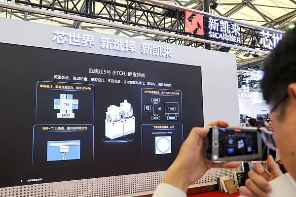
TMTPOST -- Shenzhen-based semiconductor equipment manufacturer SiCarrier Industrial Machines Co., Ltd. made a high-profile debut at SEMICON China 2025, unveiling five new semiconductor process equipment products as it seeks to challenge the dominance of foreign competitors in the industry.
The company introduced epitaxy deposition equipment (EPI), atomic layer deposition equipment (ALD), physical vapor deposition equipment (PVD), etching equipment (ETCH), and chemical vapor deposition equipment (CVD) at the event held in Shanghai from March 26 to 27.
The release drew significant interest from industry professionals, potential customers, and competitors as SiCarrier positioned itself as a rising player in China's semiconductor manufacturing sector.
SiCarrier, a state-backed enterprise with a close bond with tech giant Huawei, specializes in semiconductor equipment and electronic manufacturing tools. Corporate records show that SiCarrier Industrial was established in 2022, while its parent company, SiCarrier Technology, was founded in 2021.
Both entities are linked to entrepreneur Yu Hai and are fully owned by Shenzhen Major Industry Investment Group, which operates under the Shenzhen State-owned Assets Supervision and Administration Commission.
The company's new equipment targets key stages in semiconductor production, including epitaxy for advanced nodes and third-generation semiconductors, ALD for sub-5nm precision film deposition, and CVD for a broad range of manufacturing processes.
These segments have traditionally been dominated by multinational firms such as Applied Materials (AMAT), Tokyo Electron (TEL), and ASM.
Foreign suppliers currently control the majority of the market share for these process tools. AMAT and TEL lead in epitaxy equipment, while ALD is primarily controlled by ASM and TEL, which together hold over 60% of the market.
AMAT dominates PVD equipment with an 85% market share. SiCarrier's latest products aim to break this stranglehold, incorporating advanced reaction chamber designs that enable nanometer-level film uniformity control.
The company's next-generation photoresist coating and developing equipment, supporting nodes of 14nm and below, also represents a breakthrough in an area long controlled by foreign firms. (导读)
In addition to deposition tools, SiCarrier showcased its semiconductor inspection and metrology solutions, a critical segment for chip manufacturing quality control.
The company has developed 13 key inspection tools, including optical inspection (BFI), optical metrology (IBO), PX metrology (AFM), and power device testing (RATE-CP), with applications in logic, memory, and compound semiconductor manufacturing.
Metrology and inspection are essential for improving semiconductor yield rates, particularly as process nodes shrink to 14nm and below. Industry analysts note that a slight reduction in defect detection accuracy can significantly impact overall wafer yield, making high-precision measurement tools a crucial investment for manufacturers.
The global semiconductor inspection and metrology market reached $12.83 billion in 2023, with China‘s market at $4.36 billion, according to VLSI Research. Despite this sizable market, domestic manufacturers have struggled to compete with established foreign players.
As of 2019, Chinese firms controlled just 0.61% of the metrology sector, but this share increased to 4.34% by 2023, reflecting accelerating localization efforts.
SiCarrier has amassed over 80 patents covering optical systems, materials, and process control technologies. Recent patent filings include innovations in thermal radiation structures, process chamber designs, and electrostatic chuck technology, which addresses charge dissipation challenges in wafer processing.
The company has developed six major categories of semiconductor tools and aims to continue advancing its technological capabilities.
Shenzhen has emerged as a key hub for China's semiconductor industry, historically excelling in chip design but lagging in manufacturing.


 京公网安备 11011402013531号